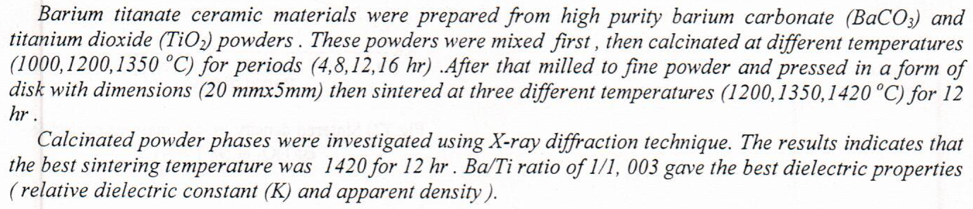
Preparation, Characterization, and Properties of Barium Titanate

It is shown that pure and 3% boron doped a-Si0.1Ge0.9:H and a-Si0.1Ge0.9:N thin films
could be prepared by flash evaporation processes. The hydrogenation and nitrogenation
are very successful in situ after depositing the films. The FT-IR analysis gave all the
known absorbing bonds of hydrogen and nitrogen with Si and Ge.
Our data showed a considerable effect of annealing temperature on the structural and
optical properties of the prepared films. The optical energy gap (Eopt.) of a-Si0.1Ge0.9
samples showed to have significant increase with annealing temperature (Ta) also the
refractive index and the real part of dielectric constant increases with Ta, however the
extinction coefficient and imaginary part of dielect
Silver Indium Aluminum Selenium AgIn1xAlxSe2 AIAS for x=01 thin films was deposited by thermal evaporation at RT and different︣︢︡ ︠︣1thickness 100 150 and 200 nm on the glass Substrate and p2Si wafer to produce AIAS/p3Si heterojunctionsolarcell4 Structural optical electrical and photovoltaicproperties6 are investigated for the samples XRD analysis reveals that all the deposited AIAS films show polycrystalline structure without any change due to increase of thickness Average diameter and roughness calculated from AFM images shows an increase in its value with increasing thickness The optical absorbance and transmittance for samples are measured using a spectrometer type UV Visible 1800 spectra1photometer to study the energy6gap The
... Show More


Nanostructural cupric oxide (CuO) films were prepared on Si and glass substrate by pulsed laser deposition technique (PLD) using laser Nd:YAG, using different laser pulses energies from 200 to 600 mJ. The X-ray diffraction pattern (XRD) of the films showed a polycrystalline structure with a monoclinic symmetry and preferred orientation toward (111) plane with nano structure. The crystallite size was increasing with increasing of laser pulse energy. Optical properties was characterized by using UV–vis spectrometer in the wave lengthrange (200-1100) nm at room temperature. The results showed that the transmission spectrum decreases with the laser pulses energy increase. Sensitivity of NO2 gas at different operating temperatures, (50°C,
... Show More (11)
(11)
ZnO thin films have been prepared by pulse laser deposition technique at room temperatures (RT). These films were deposited on GaAs substrate to form the ZnO/GaAs heterojunction solar cell. The effect of annealing temperatures at ( RT,100, 200)K on structural and optical properties of ZnO thin films has been investigated. The X-ray diffraction analysis indicated that all films have hexagonal polycrystalline structure. AFM shows that the grains uniformly distributed with homogeneous structure. The optical absorption spectra showed that all films have direct energy gap. The band gap energy of these films decreased with increasing annealing temperatures. From the electrical properties, the carriers have n-type conductivity. From
... Show More
 (1)
(1)
(1)
(1)
ABSTRACT. A new three metal complexes of La(III), Ce(IV) and UO2(II) ions have been synthesized based on a Schiff base derived from the condensation of L-histidine and anisaldehyde. All prepared compounds were characterized by different spectroscopic techniques and Density-functional theory (DFT) calculations. The complexes were proposed to have an octahedral structure based on the investigated results. The optimized shape, numbering system, and dipole moment vector of Ligand and La, Ce, and UO2 (1:1) chelates were investigated. The Schiff base ligand and complexes exhibit moderate action against all of the bacteria tested, with P. aeruginosa, Klebsiella sp., and E. faecalis respectively being the order of inhibition.
... Show More
(7)
The structural, optical properties of cupper indium gallium selenite (CuIn1-xGaxSe) have been studied. CuIn1-xGaxSe thin films for x=0.6 have been prepared by thermal evaporation technique, of 2000±20 nm thickness, with rate of deposition 2±0.1 nm/sec, on glass substrate at room temperature. Heat treatment has been carried out in the range (373-773) K for 1 hour. It demonstrated from the XRD method that all the as-deposited and annealed films have polycrystalline structure of multiphase. The optical measurement of the CIGS thin films conformed that they have, direct allowed energy gap equal to 1.7 eV. The values of some important optical parameters of the studied films such as (absorption coefficient, refractive index, extinction coeffici
... Show MoreThin films of Nb2O5 have been successfully deposited using the DC reactive magnetron sputtering technique to manufacture NH3 gas sensors. These films have been annealed at a high temperature of 800°C for one hour. The assessment of the Nb2O5 thin films structural, morphological, and electrical characteristics was carried out using several methods such as X-ray diffraction (XRD), atomic force microscopy (AFM), energy-dispersive X-ray spectroscopy (EDS), Hall effect measurements, and sensitivity assessments. The XRD analysis confirms the polycrystalline composition of the Nb2O5 thin films with a hexagonal crystal structure. Furthermore, the sensitivity, response time, and recovery time of the gas sensor were evaluated for the Nb2O5 thin film
... Show MoreCadmium sulfide and Aluminum doped CdS thin films were prepared by thermal evaporation technique in vacuum on a heated glass substrates at 373K. A comparison between the optical properties of the pure and doped films was made through measuring and analyzing the transmittance curves, and the effect of the annealing temperature on these properties were estimated. All the films were found to exhibit high transmittance in the visible/ near infrared region from 500nm to 1100nm.The optical band gap energy was found to be in the range 2.68-2.60 eV and 2.65-2.44 eV for CdS and CdS:Al respectively , with changing the annealing temperature from room temperature to 423K.Optical constants such as refractive index, extinction coefficient, and complex di
... Show More